Monday, October 5, 2020
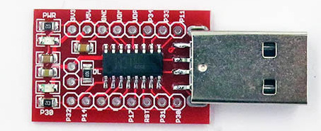
LGT8F328P EDMINI board
Thursday, September 17, 2020
Recording the Reset Pin
The AVR reset pin has many functions. In addition to being used as an external reset signal, it can be used for debugWire, and it is used for SPI and for high-voltage programming. Other than for when it is used as an external reset signal, the datasheet specifications are somewhat ambiguous. I recently started working on an updated firmware for the USBasp, and wanted to find out more details about the SPI programming mode. The image above is one of many recordings I made from programming tests of AVR MCUs.
When I first started capturing the programming signals, I observed seemingly random patterns on the MISO line before programming was enabled. Although the datasheet lists the target MISO line as being an output, it only switches to output mode after the first two bytes of the "Programming Enable" instruction, 0xAC 0x53, are received and recognized. Prior to that the pin floats, and the seemingly random patterns I observed were caused by the signals on the MOSI and SCK lines inducing a voltage on the MISO line. I enabled the pullup resistor on the programmer side in order to keep the MISO line high until the PE instruction was recognized by the target.
One of the steps in the datasheet's serial programming alorithm that doesn't make sense to me is step 2, which says, "Wait for at least 20 ms and enable Serial Programming by sending the Programming Enable serial instruction to pin MOSI." It's clear from the capture image above that a wait time of less than 100 us worked in this case. I did a number of experiments with different targets (t13, t85, m8a) with and without the CKDIV8 fuse set, and found a delay of 64 us was always sufficient. Nevertheless, I still used a 20 ms delay in the USBasp firmware.
Another observation I made was of a repeatable delay between the 8th rising edge of the SCK signal on the second byte and MISO going low. After multiple tests, I found that delay is between 2 and 3 of the target clock cyles. A close-up of the 0x53 byte shows this clearly:
The 2-3 clock ccyle delay seems to correspond with the datasheet's specification of the minimum low and high periods for the SCK signal of 2 clock cycles when the target is running at less than 12Mhz. However I found I couldn't consistently get a target running at 8MHz to enter programming mode with a SCK clock of 1.5MHz. Additional logs of the programming sequence revealed something interesting when multiple PE instructions are sent at less than 1/8th of the target clock rate, with a positive pulse on RST for synchronization. In those sequences, the delay was smaller between the 8th rising edge of the SCK signal on the second byte and MISO going low for the second and subsequent times the PE instruction is sent. It seems you need to use a slower SCK frequency to get the target into programming mode, but after that, the frequency can be increased to 1/4 of the target clock.
Using what I learned, I have implemented automatic SCK speed negotiation and a higher default SCK clock speed. The speed negotiation starts with 1.5MHz for SCK, and makes 3 attempts to enter programming mode. If that fails, the next slower speed (750kHz) is tried three times, and so on until a speed is found where the target responds. For subsequent communications with the target, the speed is doubled, since the slowest speed is only needed the first time the PE command is received after power-up. The firmware also supports a maximum SCK frequency of 3MHz, vs 1.5MHz for the original firmware.
The higher speeds don't make a large difference in flash/verify times since the overhead of the vUSB code tends to dominate beyond a SCK frequency of 750kHz or so. Reading the 8kB of flash on an ATtiny85 takes around 3 seconds. By optimizing the low-speed USB code, such as was done by Tim with u-wire, it should be possible to double that speed.
Sunday, September 6, 2020
Flashing AVRs at high speed
I've written a few bootloaders for AVR MCUs, which necessarily need to modify the flash while running. The typical 4ms to write or erase a page depends on the speed of the internal RC oscillator. Here's a quote from section 6.6.1 of the ATtiny88 datasheet:
Note that this oscillator is used to time EEPROM and Flash write accesses, and the write times will be affected accordingly. If the EEPROM or Flash are written, do not calibrate to more than 8.8 MHz. Otherwise, the EEPROM or Flash write may fail.
I wondered how running the RC oscillator well above 8.8MHz would impact erasing and writing flash In the past I read about tests showing the endurance of AVR flash and EEPROM is many times more than the spec, but I couldn't find any tests done while running the AVR at high speed. I did come across a post from an old grouch on AVRfreaks warning not to do it, so now I had to try.
The result is a program I called flashabuse, which you'll see later is a bit of a misnomer. What the program does is set OSCCAL to 255, then repeatedly erase, verify, write, and verify a page of flash. I chose to test just one page of flash for a couple reasons. First, testing all 128 pages of flash on an ATtiny88 would take much more time. The second is that I would only risk damaging one page, and an ATtiny88 with 127 good pages of flash is still useful.
The results were very positive. My little program was completing about 192 cycles per second, taking 2.6ms for each page erase or page write. I let it run for an hour and a half, so it successfully completed 1 million cycles. Not bad considering Atmel's design specification is a minimum of 10,000 cycles.
So why does the flash work fine at high speed? I think it has to do with how floating-gate flash memory works. Erasing and writing the flash requires removing and adding a charge to the floating gate using high voltages. Atmel likely uses timing margins well in excess of the 10% indicated in the datasheet, so even half the typical 4ms is more than enough to ensure error-free operation. I even think writing at high speed puts less wear on the flash because it exposes the gate to high voltages for a shorter period of time.
Addendum
Thursday, August 27, 2020
Hacker's Intro to USB hardware
Low-speed 1.5Mbps and full-speed 12Mbps USB, while more complicated than a UART, are still hacker-friendly. As the standard approaches 25 years old, I've decided to document some of the more useful highlights I've learned.
While some USB devices will have accessible PCB pads where you can probe signals, it's best to have some breakouts and pass-thru cables with test points. I've found broken micro-USB cables to be a cheap option. I cut the micro-b end off, strip the wires, and solder them to some protoboard with 4 pin headers for the ground 5V, D+ and D- connections. A crude USB voltage tester can be made with a couple silicon diodes and white or blue LED in series, powered by the 5V line. In the 20mA range, a 1N4148 has a vF of about 0.8V, so a 3.4V LED will be brightly lit if 5V is present. I've also made a custom USB-A extension cable with a section of the D+ and D- wires exposed for easy attachment of alligator clips.
Although USB power is 5V, typically at up to 500mA, the signalling is 3.3V. At the host, the data pins are pulled to ground with a resistance between 15k and 22k, so a typical host will use 18.5k Ohms. At the device, the D+(full-speed) or D-(low-speed) pin is pulled up to 3.3V to signal to the host that a device is attached. The spec (pdf) shows this being done with a 1.5k pullup to 3.6V, creates a 18.5k/20k divider, resulting in 3.6V * 0.925 or 3.33V. I've found a 10k pullup to 5V works just fine, and many devices use a 1.5k pullup to 3.3V. since the spec requires a minimum of 2.7V for detection to work. For a connected low-speed device (like a mouse), D+ will be near 0V, and D- will be near 3.3V. For a full-speed device, the polarity will be reversed. High-speed devices use low-swing 400mV signalling with both D+ and D- at 0V when idle.
The frequency counter on a multimeter can be used to tell if a device is alive, or if the host has failed to recognize it. For a device that has been enumerated by a host, the host will send a keepalive signal to the device. For a low-speed device, this is a single-ended 0 (SE0) where D- is pulled low for 1.3us every ms. Therefore, a frequency of at least 1kHz will be detected on the D- line.
You can get a USB device to reconnect without unplugging it by forcing a bus reset. This can be done by shorting the D+(full-speed) or D-(low-speed). To avoid releasing the magic smoke by accidentally shorting the wrong connection, I suggest using 100-150 ohm resistor, which is still more than sufficient to reset the bus.
Thursday, July 2, 2020
Getting started with the WCH CH551 and CH552
Instead of purchasing the bare chips for pennies at LCSC and putting together a breakout board, I bought a couple modules from Electrodragon. I had learned that the CH551, CH552, and CH554 all used the same die. I bought the CH551 and CH552 modules with the intention of eventually trying to hack them into working as a CH554.
For testing the modules, in addition to the CH554 SDK for SDCC on Linux, I've used Ch55xduino on Windows. One thing not in the Ch55xduino documentation is driver setup. The windoze version I'm using is 7E, and when I first inserted the CH551 module, I got a driver error.
Using Zadig to set the driver to libusb-win32 solved the problem.
The CH55xduino documenation also lacks pinout documentation for anything other than the reverence board. To help, I've copied the pinouts from the CH552 datahseet.
The CH55x bootloader supports DFU, which is what the CH55xduino uploader uses the first time code is uploaded to the module. Once the first sketch is uploaded, the CH55xduino core includes a CDC serial stack. With my CH551 module no longer appearing as a DFU device, I had to use Zadig again to change the CDC Serial device to use the USB Serial (CDC) driver. After that, the module appears as a COM port.
With the COM port selected in the Arduino IDE, subsequent uploads enter the bootloader by switching the baud rate to 1200bps. If no COM port is selected, the upload tool looks for a CH55x device in DFU bootloader mode. To enter the bootloader, it is necessary to pull the USB D+ pin up to 3.3V when power is applied. The Electrodragon boards have a pinout for an upload jumper, which when shorted will connect the D+ pin (P3.6/UDP)to 3.3V through a 10k resistor. On one of my modules I soldered pin headers and use a jumper to force it into upload mode. On the other, I just used a low-value (270Ohm) through-hole resistor pushed into the holes.
Currently CH55xduino is not optimized for size, with a basic blink sketch requiring 5333 bytes of flash. Officially, the CH551 is only supposed to have 10kB of available flash, so the CH55xduino overhead means less than 5kB is left for user code. The CH551 actually seems to have 12kB available for flashing user code, which I think will be plenty if the CH55xduino core gets some optimization work. Since I like to do low-level embedded coding, I'll be using SDCC from the command line most of the time. The blink example in the CH554 SDK for SDCC compiles to 700 bytes, and I was able to get that down to 232 bytes after leaving out the UART initialization in debug.c. With a bit more optimization I think I can get the blink example down to 100 bytes or so.
One small surprise I found during my testing is that the Electrodragon CH551 and CH552 modules use different pins for the user LED. On the CH551, use P3.0, working in open-drain mode so the LED light up when P3.0 is low. On the CH552, drive P1.4 high to light the LED. This is documented on the Electrodragon web site, but it is easy to forget when switching between the two modules.
I've already started to learn how to configure the standard MCS-51 UART, and have figured out how to directly manipulate the ports using the SFRs (Special Function Registers). Once I've mastered how to program these cheap little devices, I'll follow up with another blog post revealing the details.
Postscript
Thursday, June 11, 2020
A full-duplex tiny AVR software UART
I expect most AVR developers are familiar with using PWM, where the output pin is toggled at a given duty cycle, independent of the code execution. The technique behind my full-duplex UART is using the waveform generation mode so the timer/counter hardware sets the OC0A pin at the appropriate time for each bit to be transmitted. TIM0_COMPA interrupt runs after each bit is output. The ISR determines if the next bit is a 0 or a 1. For a 1 bit, TCCR0A is configured to set OC0A on compare match. For a 0 bit, TCCR0A is configured to clear OC0A on compare match. The ISR also updates OCR0A with the appropriate timer count for the next bit. To allow for simultaneous receiving, the TIM0_COMPA transmit ISR is made interruptible (the first instruction is "sei").
The receiving is handled by PCINT0, which triggers on the received start bit, and TIM0_COMPB interrupt which runs for each received bit. I wrote this ISR in assembler in order to ensure the received bit is read at the correct time, taking into consideration interrupt latency. If any other interrupts are enabled, they must be interruptible (ISR_NOBLOCK if written in C). I've implemented a two-level receive FIFO, which can be queried with the rx_data_ready() function. A byte can be read from the FIFO with rx_read().
The code is written to work with the ATtiny13, ATtiny85, and ATtiny84. Only PCINT0 is supported, which on the t84 means that the receive pin must be on PORTA. With a few modifications to the code, PCINT1 could be used for receiving on PORTB with the t84. The total time required for both the transmit and the receive ISRs is 52 cycles. Adding an average interrupt overhead of 7 cycles for each ISR means that there must be at least 66 cycles between bits. At 8Mhz this means the maximum baud rate is 8,000,000/66 = 121kbps. The lowest standard baud rate that can be used with an 8Mhz clock is 9600bps.
The wgmuart application implements an example echo program running at the default baud rate of 57.6kbps. In addition to echoing back each character received, it prints out a period '.' every second along with toggling an LED.
I've published the code on github.