Sunday, December 13, 2020

Trying to test a "ten cent" tiny ARM-M0 MCU


A few months ago, while browsing LCSC, I found a surprisingly cheap ARM M0 MCU.  At the time it was 16.6c in single-unit quantities, with no higher-volume pricing listed.  From the datasheet LCSC has posted, there was enough information in English to tell that it has 2kB RAM, 16kB flash, and runs up to 32MHz with a 1.8V to 3.6V power supply.  Although the part number suggests it may be a clone or is compatible with the STM32F030, it's not.  The part number for the STM32F030 clone is HK32F030F4P6.

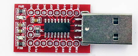
Some additional searching brought me to some Chinese web sites that advertised the chip as a 32-bit replacement for the STM8S003.  The pinout matches the STM8S003F3P6, so in theory it is a drop-in replacement for the 8S003.  Unlike the STM32F0, it has no serial bootloader, so programming has to be done via SWD.  And with no bootloader support, there's no need to be able to remap the flash from 0x0800000 to 0x0000000 like the STM32.  A small change to the linker script should be all it takes to handle that difference.  Even though I wasn't sure how or if I'd be able to program the chips, I went ahead and ordered a few of them.  I already had some TSSOP20 breakout boards, so the challenge would be in the software, and the programming hardware.

Since I'm cheap, I didn't want to buy a dedicated DAPlink programmer.  I have a STM32F103 "blue pill", so I considered converting it to a black magic probe.  But since I've been playing with the CH554 series of chips, I decided to try running CMSIS-DAP firmware on a CH552.  If you're not familiar with CMSIS-DAP and SWD, I recommend Chris Coleman's blog post.  Before I tried it with with the HK32F030MF4P6, I needed to try it with a known good target.  Since I had recently been working with a STM32F030, that's what I chose to try first.

The two main alternatives for open-source CMSIS-DAP software for downloading, running, and debugging target firmware are OpenOCD and pyOCD.  pyOCD is much simpler to use than OpenOCD; after installing it with pip, 'pyocd list' found my CH552 CMSIS-DAP:

However that's as far as I could get with pyOCD.  There seems to be a bug in the CMSIS-DAP firmware or pyOCD around the handling of the DAP_INFO message.  Fixing the bug may be a project for another day, but for the time being I decided to figure out how to use OpenOCD.

To use OpenOCD, you need to create a configuration file with information about your debug adapter and target.  It's all documented, however it's very complicated given that OpenOCD does a whole lot more than pyOCD.  It's also complicated by the fact that since the release of v0.10.0, there have been updates that have made material changes to the configuration file syntax.  I had a working configuration file on Windows that wouldn't work on Linux.  On Linux I was running OpenOCD v0.10.0-4, but on windows I was running v0.10.0-15.  After installing the xPack project OpenOCD build on Linux, the same config file worked on both Linux and Windows, which I named "cmsis-dap.cfg":

adapter driver cmsis-dap

transport select swd
adapter speed 100

swd newdap chip cpu -enable
dap create chip.dap -chain-position chip.cpu
target create chip.cpu cortex_m -dap chip.dap

init
dap info

With dupont jumpers connecting SWCLK, SWDIO, VDD, and VSS on my STM32F030 breakout board, here's the output from openocd.

After making the same connections (factoring the different pinout) to the HK32F030MF4P6, I was getting no response from the MCU.  Before connecting, I had done the usual checks for shorts and continuity, making sure all my solder connections were good.  Next I tried just connecting VDD and VSS, while I probed each pin.  Pin 2, SWDIO, was pulled high to 3V3, as was nRST.  All other pins were low, close to 0V.  The STM32F030 pulls SWDIO and nRST high too.  I tried reconnecting SWDIO and SWCLK, and connecting a line to control nRST.  I added "reset_config trst_and_srst" to my config file, and still didn't get a response.  Looking at the debug output from openocd (-d flag) shows the target isn't responding to SWD commands:

Debug: 179 99 cmsis_dap_usb.c:728 cmsis_dap_swd_read_process(): SWD ack not OK @ 0 JUNK Debug: 180 99 command.c:626 run_command(): Command 'dap init' failed with error code -4


Since the datasheet says that after reset, pin 2 functions as SWDIO, and pin 11 functions as SWCLK, I'm at a bit of an impasse.  I'll try hooking up my oscilloscope to the SWDIO and SWCLK lines to make sure the signals are clean.  I've read that in some ARM MCUs, DAP works while the device is in reset, so I'll peruse the openocd docs to figure out how to hold nRST low while communicating with the target.  And of course, suggestions are welcome.


Before I finish this post, I wanted to explain the reference to a "ten cent" MCU.  LCSC does not list volume pricing for the part, but when I searched for the manufacturer's name, "Shenzhen Hangshun Chip Technology Development", I found an article about the company.  In the article, the company president, Liu Jiping, refers to the 10c ($0.1) price.  I suspect that pricing is for quantities over 1000.  Assuming these chips can actually be programmed with a basic SWD adapter, then even paying 20c for a 20-pin, 32MHz M0 MCU looks like a good deal to me.


Read part 2 to find out how I got SWD working.


Monday, December 7, 2020

STM32 Starting Small


For software development, I often prefer to work close to the hardware.  Libraries that abstract away the hardware not only use up limited flash memory, they add to the potential sources of bugs in your code.  For a basic test of STM32 library bloat, I compiled the buttons example from my TM1638NR library in the Arduino 1.8.13 IDE using stm32duino for a STM32F030 target.  The flash required was just over 8kB, or slightly more than half of the 16kB of flash specification on the STM32F030F4P6 MCU.  While I wasn't ready to write my own tiny Arduino core for the STM32F, I was determined to find a more efficient way of programming small ARM Cortex-M devices.

After a bit of searching, looking at Bill Westfield's Miimalist ARM project, libopencm3, and other projects, I found most of what I was looking for in a series of STM32 bare metal programming posts by William Ransohoff.  However instead of using an ST-Link programmer, I decided to use a standard USB-TTL serial dongle to communicate with the ROM bootloader on the STM32.

To enable the bootloader, the STM32 boot0 pin must be pulled high during power-up. then the bootloader will wait for communication over the USART Tx and Rx lines.  On the STM32F030F4P6, the Tx line is PA9, and the Rx line is PA10.  In order reset the chip before flashing, I also connected the DTR line from my serial module to NRST (pin 4) on the MCU as shown in the following wiring diagram:

For flashing the MCU, I decided on stm32flash.  While installation on Debian Linux is as simple as, "apt install stm32flash", I had some difficulty finding a recent Windows build.  So I ended up building it myself.  Although my build defaults to 115.2kbps, I found 230.4kbps completely reliable.  At 460.8kbps and 500kbps, I encountered intermittent errors, so I stuck with 230.4kbps.  After making the necessary connections, and before flashing any code to the MCU, do a test to confirm the MCU is detected.

One thing to note about stm32flash is that it does not detect the amount of flash and RAM on the target MCU.  The numbers come from a hard-coded table based on the device ID reported.  The official flash size in kB is stored in the system ROM at address 0x1FFFF7CC.  On my STM32F030F4P6, the value read from that address is 0x0010, reflecting the spec of 16kB flash for the chip.  My testing revealed that it actually has 32kB of usable flash.

I used William's STM32F0 GPIO example as a template to create a tiny blinky example that uses less than 300 bytes of flash.  Most of that is for the vector table, which on the Cortex-M0 has 48 entries of 4 bytes each.  To save space, I embedded the reset handler in an unused part of the vector table.  Since the blinky example doesn't use any interrupts, all but the initial stack pointer at vector 0 and the reset handler at vector 1 could technically be omitted.  I plan to re-use the vector table code for other projects, so I did not prune it down to the minimum.

The blinky example will toggle PA9 at a frequency of 1Hz.  That is the UART Tx pin on the MCU, which is connected to the Rx pin on the USB-TTL dongle.  This means when the example runs, the Rx LED on the USB-TTL dongle will flash on and off.

I think my next step in Cortex-M development will be to experiment with libopencm3.  It appears to have a reasonably lightweight abstraction of GPIO and some peripherals, so it should be easier to write code that is portable across multiple different ARM MCUs.


Monday, October 5, 2020

LGT8F328P EDMINI board


Earlier this year I purchased a EDMINI board from Electrodragon.  It uses a LGT8F328P chip, which supports the AVR instruction set.  The instruction set timings and peripheral registers vary slightly from the ATmega328P, so it is not 99% compatible as claimed by Electrodragon.  I bought one to see just how compatible it is, and possibly to port some of my AVR libraries to the LGT MCU.

The module arrived in an anti-static bag, inside a padded envelope.  After connecting 5V power to the board, the D13 LED blinked on and off every second, suggesting that it comes with the Arduino blink sketch pre-loaded.  I then hooked up a USB-TTL adapter, installed the LGT board file in the Arduino IDE, and tried flashing a modified blink sketch to the board.  The upload failed, and after some debugging I found that the reset was not working on the MCU.  Neither pressing and holding the reset button nor grounding RST would reset the board.  After contacting Electrodragon, Chao agreed replace the board, with two new boards.  He told me that they see a higher than average failure rate with the LGT8F328P chips.

In addition to Chao's frank comment about reliability, another concern I had about the LGT parts was the lack of markings on the chip.  I suspect LGT sells the parts without markings so vendors can label them with their own brand.  This also makes it easier for more nefarious manufacturers to label them as an ATmega328p.  

When the new boards arrived, the first thing I did was make sure the reset button worked.  After pressing reset the LED flashes quickly three times for the bootloader, and then flashes on and off every second.  However when I tried uploading sketch using the Arduino IDE, the upload still failed.  After some more debugging, I found I could upload if I pressed the reset button just before uploading.  This meant the bootloader was working, but auto-reset (toggling the DTR line) was not.  These boards use the same auto-reset circuit as an Arduino Pro Mini:

A negative pulse on DTR will cause a voltage drop on RST, which is supposed to reset the target.  When the target power is 5V and 3V3 TTL signals are used, toggling DTR will cause RST to drop from 5V to about 1.7V (5 - 3.3).  With the ATmega328P and most other AVR MCUs, 2V is low enough to reset the chip.  The LGT8F328P, however requires a lower voltage to reset.  In some situations this can be a good thing, as it means the LGT MCU is less likely to reset due to electromagnetic interference.

The EDMINI board has a 3V3 regulator which can be selected by a solder jumper.  This is mentioned on the Electrodragon site, but it is not clearly documented which pads need to be shorted to switch from 5V to 3V3.  After a bit of debugging I was able to run the board at 3V3, and was able to use the auto-reset feature.

I do most of my AVR development using command line tools, not the Arduino IDE.  I compiled a small program that toggles every pin on PORTB using avr-gcc 5.4.0, and flashed it to the EDMINI board using avrdude.  Nothing happened.  Since the Arduino blink sketch worked, I know that the LED on PB5 was working.  My conclusion is that the LGT Arduino core must do some setup to enable PORTB.  This is common on modern MCUs such as the ARM Cortex, but on AVRs like the ATmega328p, writing 255 to the PORTB and DDRB registers is all it takes to drive every pin on port B high.

I won't be doing any development work with the LGT MCUs.  Although they are cheaper and can run a bit faster than authentic AVR parts, their compatibility is rather limited.  Any code that relies on the standard AVR instruction set timing, such as my picoUART library, will not work.  The 8F328P cannot be programed with a USBasp, as the native programming interface is SWD, not Atmel's SPI-based protocol.  For a cheap and powerful MCU, the CH551 looks much more interesting.

Thursday, September 17, 2020

Recording the Reset Pin


The AVR reset pin has many functions.  In addition to being used as an external reset signal, it can be used for debugWire, and it is used for SPI and for high-voltage programming. Other than for when it is used as an external reset signal, the datasheet specifications are somewhat ambiguous.  I recently started working on an updated firmware for the USBasp, and wanted to find out more details about the SPI programming mode.  The image above is one of many recordings I made from programming tests of AVR MCUs.

When I first started capturing the programming signals, I observed seemingly random patterns on the MISO line before programming was enabled.  Although the datasheet lists the target MISO line as being an output, it only switches to output mode after the first two bytes of the "Programming Enable" instruction, 0xAC 0x53, are received and recognized.  Prior to that the pin floats, and the seemingly random patterns I observed were caused by the signals on the MOSI and SCK lines inducing a voltage on the MISO line.  I enabled the pullup resistor on the programmer side in order to keep the MISO line high until the PE instruction was recognized by the target.

One of the steps in the datasheet's serial programming alorithm that doesn't make sense to me is step 2, which says, "Wait for at least 20 ms and enable Serial Programming by sending the Programming Enable serial instruction to pin MOSI."  It's clear from the capture image above that a wait time of less than 100 us worked in this case.  I did a number of experiments with different targets (t13, t85, m8a) with and without the CKDIV8 fuse set, and found a delay of 64 us was always sufficient.  Nevertheless, I still used a 20 ms delay in the USBasp firmware.

Another observation I made was of a repeatable delay between the 8th rising edge of the SCK signal on the second byte and MISO going low.  After multiple tests, I found that delay is between 2 and 3 of the target clock cyles.  A close-up of the 0x53 byte shows this clearly:


The 2-3 clock ccyle delay seems to correspond with the datasheet's specification of the minimum low and high periods for the SCK signal of 2 clock cycles when the target is running at less than 12Mhz.  However I found I couldn't consistently get a target running at 8MHz to enter programming mode with a SCK clock of 1.5MHz.  Additional logs of the programming sequence revealed something interesting when multiple PE instructions are sent at less than 1/8th of the target clock rate, with a positive pulse on RST for synchronization.  In those sequences, the delay was smaller between the 8th rising edge of the SCK signal on the second byte and MISO going low for the second and subsequent times the PE instruction is sent.  It seems you need to use a slower SCK frequency to get the target into programming mode, but after that, the frequency can be increased to 1/4 of the target clock.

Using what I learned, I have implemented automatic SCK speed negotiation and a higher default SCK clock speed.  The speed negotiation starts with 1.5MHz for SCK, and makes 3 attempts to enter programming mode.  If that fails, the next slower speed (750kHz) is tried three times, and so on until a speed is found where the target responds.  For subsequent communications with the target, the speed is doubled, since the slowest speed is only needed the first time the PE command is received after power-up.  The firmware also supports a maximum SCK frequency of 3MHz, vs 1.5MHz for the original firmware.

The higher speeds don't make a large difference in flash/verify times since the overhead of the vUSB code tends to dominate beyond a SCK frequency of 750kHz or so.  Reading the 8kB of flash on an ATtiny85 takes around 3 seconds.  By optimizing the low-speed USB code, such as was done by Tim with u-wire, it should be possible to double that speed.

Sunday, September 6, 2020

Flashing AVRs at high speed


I've written a few bootloaders for AVR MCUs, which necessarily need to modify the flash while running.  The typical 4ms to write or erase a page depends on the speed of the internal RC oscillator.  Here's a quote from section 6.6.1 of the ATtiny88 datasheet:

Note that this oscillator is used to time EEPROM and Flash write accesses, and the write times will be affected accordingly. If the EEPROM or Flash are written, do not calibrate to more than 8.8 MHz. Otherwise, the EEPROM or Flash write may fail.

I wondered how running the RC oscillator well above 8.8MHz would impact erasing and writing flash  In the past I read about tests showing the endurance of AVR flash and EEPROM is many times more than the spec, but I couldn't find any tests done while running the AVR at high speed.  I did come across a post from an old grouch on AVRfreaks warning not to do it, so now I had to try.

The result is a program I called flashabuse, which you'll see later is a bit of a misnomer.  What the program does is set OSCCAL to 255, then repeatedly erase, verify, write, and verify a page of flash.  I chose to test just one page of flash for a couple reasons.  First, testing all 128 pages of flash on an ATtiny88 would take much more time.  The second is that I would only risk damaging one page, and an ATtiny88 with 127 good pages of flash is still useful.

The results were very positive.  My little program was completing about 192 cycles per second, taking 2.6ms for each page erase or page write.  I let it run for an hour and a half, so it successfully completed 1 million cycles.  Not bad considering Atmel's design specification is a minimum of 10,000 cycles.

So why does the flash work fine at high speed?  I think it has to do with how floating-gate flash memory works.  Erasing and writing the flash requires removing and adding a charge to the floating gate using high voltages.  Atmel likely uses timing margins well in excess of the 10% indicated in the datasheet, so even half the typical 4ms is more than enough to ensure error-free operation.  I even think writing at high speed puts less wear on the flash because it exposes the gate to high voltages for a shorter period of time.

Addendum

I received some feedback questioning whether the faster write time may reduce retention due to reduced charge on the floating gate.  As I mentioned above, Atmel likely used a very large timing margin when designing the flash memory.  Chris Lamont, who tested flash retention on a PIC32, stated that retention failure is "extremely unlikely".

The retention specs for the ATtiny88 are, "20 years at 85°C / 100 years at 25°C".  As this Micron technical note (PDF) shows, retention specs are based on models, not actual testing.  Micron's JESD47I PCHTDR testing is done at 125C for 1000 hours, and requires 0 failures.  TEKMOS states, "As a very rough rule of thumb, the data retention time halves for every 10C rise in temperature."  Extrapolating from a 100-year retention at 25C, retention at 255C, a typical reflow soldering peak temperature, would be only 6 minutes.

In an attempt to show that retention is not impacted by repeated fast flashing, I performed two additional tests.  For the first test, I baked the subject MCU for 12 hours at 150C, then performed 100,000 fast write/erase cycles.  Next, 0x55 was written to the test page, and repeatedly verified for 2 hours.  This test passed with no errors.  For the second test, I filled the 8kB of flash with zeros to put a charge on the floating gate for every bit.  I then baked the subject MCU for 12 hours at 150C, then verified that all bits remained at zero.  This test passed with all 65,536 bits reading zero.  I did, however have a failure of one solder joint, likely due to the stress of thermal cycling.

For those who are particularly concerned paranoid about flash retention, one solution is refereshing the flash.  For an AVR MCU, it would be simple to refesh the flash on every bootup with a small segment of code in .init1.  The code would copy each page into the page buffer, then perform a write on the page.  This would refresh all the 0 bits, and extend the retention life for another 20 to 100 years.

Thursday, August 27, 2020

Hacker's Intro to USB hardware


Low-speed 1.5Mbps and full-speed 12Mbps USB, while more complicated than a UART, are still hacker-friendly.  As the standard approaches 25 years old, I've decided to document some of the more useful highlights I've learned.

While some USB devices will have accessible PCB pads where you can probe signals, it's best to have some breakouts and pass-thru cables with test points.  I've found broken micro-USB cables to be a cheap option.  I cut the micro-b end off, strip the wires, and solder them to some protoboard with 4 pin headers for the ground 5V, D+ and D- connections.  A crude USB voltage tester can be made with a couple silicon diodes and white or blue LED in series, powered by the 5V line.  In the 20mA range, a 1N4148 has a vF of about 0.8V, so a 3.4V LED will be brightly lit if 5V is present.  I've also made a custom USB-A extension cable with a section of the D+ and D- wires exposed for easy attachment of alligator clips.

Although USB power is 5V, typically at up to 500mA, the signalling is 3.3V.  At the host, the data pins are pulled to ground with a resistance between 15k and 22k, so a typical host will use 18.5k Ohms.  At the device, the D+(full-speed) or D-(low-speed) pin is pulled up to 3.3V to signal to the host that a device is attached.  The spec (pdf) shows this being done with a 1.5k pullup to 3.6V, creates a 18.5k/20k divider, resulting in 3.6V * 0.925 or 3.33V. I've found a 10k pullup to 5V works just fine, and many devices use a 1.5k pullup to 3.3V. since the spec requires a minimum of 2.7V for detection to work.  For a connected low-speed device (like a mouse), D+ will be near 0V, and D- will be near 3.3V.  For a full-speed device, the polarity will be reversed.  High-speed devices use low-swing 400mV signalling with both D+ and D- at 0V when idle.

The frequency counter on a multimeter can be used to tell if a device is alive, or if the host has failed to recognize it.  For a device that has been enumerated by a host, the host will send a keepalive signal to the device.  For a low-speed device, this is a single-ended 0 (SE0) where D- is pulled low for 1.3us every ms.  Therefore, a frequency of at least 1kHz will be detected on the D- line.

You can get a USB device to reconnect without unplugging it by forcing a bus reset.  This can be done by shorting the D+(full-speed) or D-(low-speed).  To avoid releasing the magic smoke by accidentally shorting the wrong connection, I suggest using 100-150 ohm resistor, which is still more than sufficient to reset the bus.

Thursday, July 2, 2020

Getting started with the WCH CH551 and CH552

When I first read about the CH554 series of MCUs, I thought it would be interesting to test out some day.  Part of the attraction is that it's based on the 8051, which is a well-documented an widely used architecture.  The first assembly language I learned almost 40 years ago was for the 6502, so learning to program the 8-bit CISC should be relatively easy.

Instead of purchasing the bare chips for pennies at LCSC and putting together a breakout board, I bought a couple modules from Electrodragon.  I had learned that the CH551, CH552, and CH554 all used the same die.  I bought the CH551 and CH552 modules with the intention of eventually trying to hack them into working as a CH554.

For testing the modules, in addition to the CH554 SDK for SDCC on Linux, I've used Ch55xduino on Windows.  One thing not in the Ch55xduino documentation is driver setup.  The windoze version I'm using is 7E, and when I first inserted the CH551 module, I got a driver error.

Using Zadig to set the driver to libusb-win32 solved the problem.

The CH55xduino documenation also lacks pinout documentation for anything other than the reverence board.  To help, I've copied the pinouts from the CH552 datahseet.


The CH55x bootloader supports DFU, which is what the CH55xduino uploader uses the first time code is uploaded to the module.  Once the first sketch is uploaded, the CH55xduino core includes a CDC serial stack.  With my CH551 module no longer appearing as a DFU device, I had to use Zadig again to change the CDC Serial device to use the USB Serial (CDC) driver.  After that, the module appears as a COM port.

With the COM port selected in the Arduino IDE, subsequent uploads enter the bootloader by switching the baud rate to 1200bps.  If no COM port is selected, the upload tool looks for a CH55x device in DFU bootloader mode.  To enter the bootloader, it is necessary to pull the USB D+ pin up to 3.3V when power is applied.  The Electrodragon boards have a pinout for an upload jumper, which when shorted will connect the D+ pin (P3.6/UDP)to 3.3V through a 10k resistor.  On one of my modules I soldered pin headers and use a jumper to force it into upload mode.  On the other, I just used a low-value (270Ohm) through-hole resistor pushed into the holes.

Currently CH55xduino is not optimized for size, with a basic blink sketch requiring 5333 bytes of flash.  Officially, the CH551 is only supposed to have 10kB of available flash, so the CH55xduino overhead means less than 5kB is left for user code.  The CH551 actually seems to have 12kB available for flashing user code, which I think will be plenty if the CH55xduino core gets some optimization work.  Since I like to do low-level embedded coding, I'll be using SDCC from the command line most of the time.  The blink example in the CH554 SDK for SDCC compiles to 700 bytes, and I was able to get that down to 232 bytes after leaving out the UART initialization in debug.c. With a bit more optimization I think I can get the blink example down to 100 bytes or so.

One small surprise I found during my testing is that the Electrodragon CH551 and CH552 modules use different pins for the user LED.  On the CH551, use P3.0, working in open-drain mode so the LED light up when P3.0 is low.  On the CH552, drive P1.4 high to light the LED.  This is documented on the Electrodragon web site, but it is easy to forget when switching between the two modules.

I've already started to learn how to configure the standard MCS-51 UART, and have figured out how to directly manipulate the ports using the SFRs (Special Function Registers).   Once I've mastered how to program these cheap little devices, I'll follow up with another blog post revealing the details.

Postscript

I recently found out that these modules do not fit well in a solderless breadboard.  The row spacing for the 0.1" headers on the CH551 is about 0.47", so the pins have to bend out slightly to plug into the breadboard.  On the CH552 module, the row spacing is about 0.52", so the pins have to bend out slightly to fit.

Thursday, June 11, 2020

A full-duplex tiny AVR software UART

I've written a few software UARTs for AVR MCUs.  All of them have bit-banged the output, using cycle-counted assembler busy loops to time the output of each bit.  The code requires interrupts to be disabled to ensure accurate timing between bits.  This makes it impossible to receive data at the same time as it is being transmitted, and therefore the bit-banged implementations have been half-duplex.  By using the waveform generator of the timer/counter in many AVR MCUs, I've found a way to implement a full-duplex UART, which can simultaneously send and receive at up to 115kbps when the MCU is clocked at 8Mhz.

I expect most AVR developers are familiar with using PWM, where the output pin is toggled at a given duty cycle, independent of the code execution.  The technique behind my full-duplex UART is using the waveform generation mode so the timer/counter hardware sets the OC0A pin at the appropriate time for each bit to be transmitted.  TIM0_COMPA interrupt runs after each bit is output.  The ISR determines if the next bit is a 0 or a 1.  For a 1 bit, TCCR0A is configured to set OC0A on compare match.  For a 0 bit, TCCR0A is configured to clear OC0A on compare match.  The ISR also updates OCR0A with the appropriate timer count for the next bit.  To allow for simultaneous receiving, the TIM0_COMPA transmit ISR is made interruptible (the first instruction is "sei").

The receiving is handled by PCINT0, which triggers on the received start bit, and TIM0_COMPB interrupt which runs for each received bit.  I wrote this ISR in assembler in order to ensure the received bit is read at the correct time, taking into consideration interrupt latency.  If any other interrupts are enabled, they must be interruptible (ISR_NOBLOCK if written in C).  I've implemented a two-level receive FIFO, which can be queried with the rx_data_ready() function.  A byte can be read from the FIFO with rx_read().

The code is written to work with the ATtiny13, ATtiny85, and ATtiny84.  Only PCINT0 is supported, which on the t84 means that the receive pin must be on PORTA.  With a few modifications to the code, PCINT1 could be used for receiving on PORTB with the t84.  The total time required for both the transmit and the receive ISRs is 52 cycles.  Adding an average interrupt overhead of 7 cycles for each ISR means that there must be at least 66 cycles between bits.  At 8Mhz this means the maximum baud rate is 8,000,000/66 = 121kbps.  The lowest standard baud rate that can be used with an 8Mhz clock is 9600bps.

The wgmuart application implements an example echo program running at the default baud rate of 57.6kbps.  In addition to echoing back each character received, it prints out a period '.' every second along with toggling an LED.


I've published the code on github.

Monday, April 27, 2020

Measuring AVR interrupt latency

One thing I like about AVR MCUs is that their datasheets are relatively short and simple.  It's also one of the things I don't like, because the datasheets often lack important details.  Understanding external interrupt latency is one things that is lacking complete and clear details.  I decided to investigate the interrupt latency of the ATtiny13 and the ATtiny85.  The datasheet's description of interrupt response time and external interrupts is identical for both parts.

Interrupt Response Time

The ATtiny13 datasheet section 4.7.1, under the heading "Interrupt Response Time", says, "The interrupt execution response for all the enabled AVR interrupts is four clock cycles minimum. After four clock cycles the Program Vector address for the actual interrupt handling routine is executed. [...] The vector is normally a jump to the interrupt routine, and this jump takes three clock cycles. [...] If an interrupt occurs when the MCU is in sleep mode, the interrupt execution response time is increased by four clock cycles."

While section 4.7.1 is reasonably detailed, it has one significant error, and another important omission.  The error is the sentence, "The vector is normally a jump to the interrupt routine, and this jump takes three clock cycles".  All AVRs with less than 8KB of flash, like the ATtiny13, have no jump instruction.  They only have a relative jump "rjmp", which takes two clock cycles.  This is obviously a copy/paste error from the datasheet of an AVR with  more than 8KB of flash.  Anyone familiar with the AVR instruction set would likely catch this simple error. The omission from section 4.7.1 is much harder to recognize until you carefully examine section 9.2 and figure 9-1 in the datasheet.

Figure 9-1 shows a circuit which appears to add a latency of two clock cycles to pin change interrupts.  There is no written description for the circuit, and the external interrupt details in section 9.2 of the datasheet state, "Pin change interrupts on PCINT[5:0] are detected asynchronously."  Since pin change interrupts can be used to wake the part from power-down sleep mode when all clocks are disabled, they must be detected asynchronously during power-down sleep.  To determine when they are detected synchronously requires testing.

To test the interrupt latency I wrote a program in assembler that can generate low pulses of different lengths using PWM.  I chose not to write the program in C because I want to be able to measure the interrupt latency down to a single cycle.  On the t13, PB1 is the pin for INT0, PCINT1, and  OC0B.  By using OC0B to generate a low pulse on PB1, I'll be able to trigger INT0 and PCINT1 without any external connections.  When the interrupt is triggered, it should take four cycles to execute the code at the interrupt vector.  That code is an rjmp to the interrupt function, and that rjmp takes two additional clock cycles.  For the best-case latency, the first instruction in the interrupt function will execute six cycles after the interrupt is triggered.

The first instruction of the interrupt function checks the state of the pin that triggered the interrupt (the "sbic" instruction).  If the pin is low, it skips the next instruction, then goes into an infinite loop.  If the pin is high, it toggles the LED pin.  Since the PWM is configured to generate a low pulse, if the pulse has ended before the sbic, the LED will light up to indicate the interrupt response time was too slow.  The length of the pulse is one cycle longer than the value stored in OCR0B, which is done at lines 28 and 29.  My testing consisted mainly of modifying the OCR0B value, then building and flashing the modified code to the AVR.

Results

As expected INT0 latency is 4 clock cycles from the end of the currently executing instruction.  This means that if the interrupt occurs during the first cycle of a call instruction which takes 3 cycles, the interrupt response time will be 6 cycles.  For pin change interrupts, the latency is 6 cycles, indicating the synchronizer circuit adds 2 cycles of latency.  In idle sleep mode, both INT0 and PCINT latency is 8 cycles, indicating pin change interrupts operate asynchronously when the CPU clock is not running.

Wednesday, April 8, 2020

Better asserts in C with link-time optimization

I've been a fan of link-time optimization for several years.  I've been a fan of efficient programming for even longer.  I was an early fan of C++ because features like function overloading made it easier to move decisions done at run-time in C to compile-time with C++.  As C++ has become more complex over the decades, I've become less of a C++ fan, and appreciate the simplicity of C.

For small embedded systems like 8-bit AVRs and ARM M0, run-time error checking with assert() has minimal usefulness compared to UNIX, where a a core dump will help pinpoint the error location and the state of the program at the time of the error.  Even if the usability problems were solved, real-time embedded systems may not be able to afford the performance costs of run-time error checking.

Both C++ and C support static assertions.   Anyone who has tried to use static_assert likely has encountered "expression in static assertion is not constant" errors for anything but the simplest of checks.  The limitations of static_assert is well documented elsewhere, so I will not go into further details in this post.

I had long understood that LTO allowed the compiler to evaluate expressions in code at build time,  I never realized it's potential for static error checking.  The idea came to me when looking at a fellow embedded developer's code for fast Arduino digital IO.  In particular, Bill's code introduced me to the gcc error function attribute.  The documentation describes the attribute as follows:

  • If the error or warning attribute is used on a function declaration and a call to such a function is not eliminated through dead code elimination or other optimizations, an error or warning (respectively) that includes message is diagnosed.  This is useful for compile-time checking ...
Despite the fact that it seems the error attribute was introduced to address some of the limitations of static asserts, it doesn't seem to be commonly used.  After some experimentation, I came up with a basic example.
pll.c:
__attribute((error("")))
void constraint_error(char * details);

volatile unsigned pll_mult;


void set_pll_mult(unsigned multiplier)
{
    if (multiplier > 8) constraint_error("multlier out of range");
    pll_mult = multiplier;
}

main.c:
extern void set_pll_mult(unsigned multiplier);

int main()
{
    set_pll_mult(9);
}

$ gcc -Os -flto -o main *.c
In function 'set_pll_mult.constprop',
    inlined from 'main' at main.c:6:5:
pll.c:9:25: error: call to 'constraint_error' declared with attribute error:
     if (multiplier > 8) constraint_error("multlier out of range");
                         ^
When set_pll_mult() is called with an argument greater than 8, a compile error occurs.  When it is compiled with a valid multiplier, the "if (multiplier > 8)" statement is eliminated by the optimizer.  One drawback to the technique is that the caller (main.c in this case) is not identified when the called function is not inlined.  Increasing the optimization level to O3 may help to get the function inlined.

Wednesday, February 12, 2020

Building a better bit-bang UART - picoUART

Over the past years, one of my most popular blog posts has been a soft UART for AVR MCUs.  I've seen variations of my soft UART code used in other projects.  When MicroCore recently integrated a modified version of my old bit-bang UART code, it got me thinking about how I could improve it.

There were a few limitations to my earlier UART code.  One was that it didn't support baud rates below 19.2kbps at 8Mhz or baud rates below 38.4kbps at 16Mhz.  It was also problematic for people that tried to integrate it into C/C++ libraries, as the code was written in AVR assembler.  Another problem that was recently brought to my attention by James Sleeman, was that the UART receive didn't work well at moderately high baud rates such as 57.6kbps.  Since my AVR skills had improved over time, I was confident I could make tangible improvements to the code I wrote in 2014.


The screen shot above is from picoUART running on an ATtiny13, at a baud rate of 230.4kbps.  The new UART has several improvements over my old code.  To understand the improvements, it helps to understand how an asynchronous serial TTL UART works first.


Most embedded systems use 81N communication, which means 8 data bits, 1 stop bit, and no parity.  Each frame begins with a low start bit, so the total frame is 1 start bit + 8 data bits + 1 stop bit for a total of 10 bits.  Frames can be sent back-to-back with no idle time between them.  The data is sent at a fixed baud rate, and when either the receiver or transmitter varies from the chosen baud rate, errors can occur.

When it comes to the timing error tolerance of asynchronous serial communications, I've often read that somewhere between 2% and 3.5% timing error is acceptable.  I've also read many "experts" claim that a micro-controller needs an accurate external crystal oscillator in order to avoid UART timing errors.  The truth is that UART timing can be off by a total of over 5% without encountering errors.  By total, I mean the sum of the errors for both ends, so if a transmitter is 2% fast, and the receiver is 2% slow, the 81N data frames can still be received error-free.  The timing on a USB-TTL UART adapter is usually accurate to within 0.1%, so if I am sending data from an AVR that is running 3% slow, my PL2303HX adapter still receives it error-free.

If a frame is being transmitted at 57.6kbps, each bit needs to last 1000/57.6 = 17.36us.  That means 17.36us after bringing the line low for the start bit, the least significant bit needs to be sent.  A receiver will wait for the start bit to begin, wait another 17.36, and then wait for the middle of the first bit to sample the line.  If the line is high, the bit is a 1, and it it is low, the bit is a zero.  So the receiver will sample the first bit 1.5 * 17.36 = 26.04us after the line goes low to signal the start bit.  The last(8th) bit will be sampled after 8.5 *17.36 = 147.56us.  If the transmitter is to slow, and is still transmitting the 7th bit, it will cause a communication error, as the receiver will interpret the 7th bit as actually being the 8th bit.  If the transmitter is still sending the 7th bit after 147.56us, then it is sending at 8/8.5 or 0.941 * 57.6 = 54.2kbps.  Since many UARTs check for a valid stop bit, the maximum timing error is usually 9/9.5 or 94.7% of the baud rate.

The transmit timing of my earlier soft UART implementations is accurate to within 3 clock cycles.  This was each iteration of the delay loop takes 3 clock cycles - one for decrement and two for the branch:
    ldi delayArg, TXDELAY
TxDelay:
    dec delayArg
    brne TxDelay

And since delayArg is an 8-bit register, the maximum delay added to the transmission of each bit is 2^8 * 3 = 768 cycles.  On a MCU running at 8Mhz, that limited the lowest baud rate to around 8000/768 or 10.4kbps.  To allow for lower bit rates, picoUART needed to support longer delays.  I also wanted to support more accurate timing, so picoUART uses __builtin_avr_delay_cycles during the transmission of each bit.  The exact number of cycles to wait is calculated by some inline functions, which is a better way of doing the calculations than the macros I had used before.  Writing picoUART in C made the timing calculations more difficult, since compiler has some flexibility in how the code is compiled to AVR machine instructions.  In order to get avr-gcc to generate the exact sequence of instructions that I wanted, I had to use one inline asm statement.  When I used a C "while" loop instead of the asm goto "brne" instruction, the loop was one cycle longer due to a superfluous compare instruction.  Future versions of the compiler may have improved optimization and omit the compare, which would slightly impact the timing.

As with the transmit code, picoUART's receive code is accurate to within one cycle.  Unlike my earlier UART code, picoUART returns after reading the 8th bit instead of waiting for the stop bit.  Because of this change, picoUART begins by waiting for the line to be high before waiting for the start bit.  Without the initial wait for high, back-to-back calls to purx() could lead an error when the 8th bit of one frame is 0(low) and gets interpreted as the start bit of the next frame.  This change approximately triples the amount of time for the AVR to process each byte in a continuous stream of data.

My earlier UART code had two incompatible versions.  One version used open-drain communication, where the transmit line is pulled high by an external resistor, and pulled low by the AVR.  This version supported using a single wire for both receive and transmit.  While it also worked with separate pins, some users found it inconvenient to add the pull-up resistor.  Instead they would choose the "push-pull" version, where the AVR drives the line high and pulls it low.  With picoUART a single version works for both use cases, because it works in "push-pull" mode only during transmit.  When not actively transmitting, the IO pin is set to input mode with the internal pull-up activated.

I've tried to help both the noobs and experienced AVR developers.  The noob can download a release zip file to add as an Arduino library.  If you are an old AVR developer like me that prefers a keyboard over a mouse, you'll find a basic Makefile with the echo example.  The default baud rate is 115.2kbps, although it is capable of accurate timing at much higher speeds such as 1mbps for an AVR running at 8Mhz.  The default transmit is on PB0, with PB1 for receive.  The defaults can be changed in pu_config.h, or with build flags like "-DPU_BAUD_RATE=230400L".

Saturday, January 11, 2020

Picoboot v3 with autobaud and timeout

Today I released v3 beta2 of picoboot.  Like the last release of picoboot, it takes up only 256 bytes, which is the minimum bootloader size supported on the ATmega88 and ATmega168.  This means picoboot will free up 256 bytes of flash if you currently use Optiboot.  Without any potential benefit from reduced size, this release focused on robustness and speed.


The above screen shot shows reading the 16kB flash memory of an ATmega168 in 1.32 seconds.  Using 500kbps instead of 250 will read the flash in under one second, and will read 32kB of flash from an ATmega328 in two seconds.  Not only is it fast, it is reliable, with no errors using CH340G and CP2102 adapters under Windows, and PL2303HX adapters under Linux.  So as long as your serial driver supports 250 or 500kbps and doesn't round them down to 230,400 and 460,800, you can have reliable and high speed uploading and verify of code on ATmega MCUs.

Earlier versions of picoboot supported a bootloader toggle mode, where resetting the MCU once entered the bootloader, and resetting again ran the application code.  I designed this with boards that don't support the auto-reset functionality of the Arduino bootloader.  However this turned out to be problematic with some boards that do have auto-reset, where picoboot could sometimes toggle out of bootloader mode when it was supposed to enter bootloader mode.  With v3, picoboot now implements a timeout where it will wait for a few seconds and if no communication is received from avrdude, the bootloader will exit.

Like the previous versions, picoboot does not use the watchdog timer, and will not impact application code that uses the watchdog reset.  To make picoboot useful for use with a standalone AVR on a breadboard, it does not rely on a user LED on PB5 to indicate bootloader activity.  Instead, when the bootloader starts, it lowers the TXD line (PD1).  This will light the RX LED on the attached serial adapter.  If the bootloader times out, PD1 will be left floating before the bootloader exits.

My recommended baud rate for picoboot is 250kbps.  This baud rate results in 0 timing error with the AVR USART when used with the common clock rates of 8, 12, and 16Mhz, as well as the less-common 20Mhz.  The faster 500kbps also results in 0 timing error with the USART, however poor design of some serial adapters  makes the higher speeds more susceptible to noise, particularly when long wires are used to connect to the AVR.  I didn't encounter problems at 500kbps, but I was a bit surprised by how much noise I saw on my oscilloscope when testing a CP2102.

If you are using the Arduino IDE rather than the command line, I explained how to change the boards.txt file in my blog post about picoboot v1.

I plan to test v3 beta 2 for about a month, so expect the final v3 in early February.  In addition to further testing on the mega168 and mega328, I'll test the mega88.  If there is enough interest in a build for the mega8, I'll look into supporting it too.